MyCompetitiveExams Logo MyCompetitiveExams
Search 1,140+ Questions
Chapters, formulas, speed tricks
→
⚡ Brahmastra NEET 2027
720 MARKS

Dynamic 180-question full-length simulator mixed dynamically from all 6 years for 2027 & 2026 aspirants.

Launch Brahmastra 2027 Test →
Start Practice →
100% Free · No Login Required
Q.156 Physics ⭐ 360° Option Elimination Active
Vault ↗

NEET 2020 Physics Question 156 Solution

Topic: Semiconductor Electronics: Materials, Devices and Simple Circuits · Official NTA Booklet Code E1
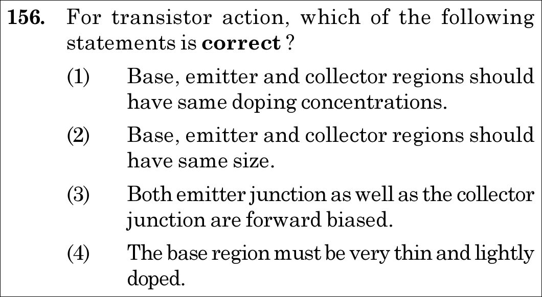
NEET 2020 Physics Question 156: Transistor Structure Requirements: Base Region Must be Very Thin and Lightly Doped

Question

For transistor action, which of the following statements is correct?

  1. (1)Base, emitter and collector regions should have same doping concentrations.
  2. (2)Base, emitter and collector regions should have same size.
  3. (3)Both emitter junction as well as the collector junction are forward biased.
  4. (4)The base region must be very thin and lightly doped.
✓
Verified Against NTA Final Answer Key
Option (4) : The base region must be very thin and lightly doped.
📚 Semiconductor Electronics: Materials, Devices and Simple Circuits Easy
📋 Given Parameters & Problem Setup
Device Bipolar Junction Transistor (BJT: n-p-n or p-n-p)
Functional Regimes Transistor action in active mode (amplification)
Question Objective Identify the CORRECT statement regarding transistor structural requirements
⚡

The 30-Second Exam Hall Shortcut: ⚡ "Transistor Action: Base Must Be Extremely THIN and LIGHTLY DOPED!"

⏱️ 20 seconds

For proper transistor action, majority carriers emitted by the emitter must pass through the base into the collector without recombining. To minimize base recombination loss (< 5%), the base region MUST BE EXTREMELY THIN (~few micrometers) AND VERY LIGHTLY DOPED! Emitter is heavily doped, collector is moderately doped. Statement (4) is 100% correct! Mark Option (4) in 5 seconds.

1 Doping profile: Emitter (heavily doped) > Collector (moderately doped) > Base (very lightly doped).
2 Physical size: Collector (largest) > Emitter (moderate) > Base (extremely thin).
3 Active bias: Emitter-base is forward biased; Collector-base is reverse biased.
4 Thus, options (1), (2), and (3) are all false.
5 Statement (4) is correct: "The base region must be very thin and lightly doped."
6 Select Option (4).
🛡️
Why You Can 100% Trust This Shortcut: NCERT Physics · Semiconductor Electronics (Bipolar Junction Transistor: Structure and Action)
📐

Step-by-Step Rigorous Workflow & Mathematical Proof

Step 1

Structural Architecture of a Transistor

A junction transistor has three distinct doped regions: 1. Emitter: Supplies majority charge carriers; it is moderately sized and HEAVILY DOPED. 2. Base: The central connecting region; it is EXTREMELY THIN (~few micrometers) and VERY LIGHTLY DOPED. 3. Collector: Collects carriers passing through base; it is physically the LARGEST in size (to dissipate heat) and MODERATELY DOPED.

Step 2

Evaluate Statement (1) and (2)

- Statement (1) claims all regions have same doping: False, doping order is Emitter > Collector > Base. - Statement (2) claims all regions have same size: False, size order is Collector > Emitter > Base.

Step 3

Evaluate Statement (3): Biasing in Active Mode

For normal transistor action (active amplification mode): - The emitter-base junction must be FORWARD BIASED. - The collector-base junction must be REVERSE BIASED. Statement (3) falsely claims both junctions are forward biased (which is the saturation regime, not normal active transistor action).

Step 4

Evaluate Statement (4): Role of Thin, Lightly Doped Base

If the base were thick or heavily doped, most majority carriers injected from the emitter would recombine in the base and never reach the collector. The thin and lightly doped base ensures that only ~2-5% of carriers recombine (IBI_B is very small), allowing >95% to cross into the collector (IC≈IEI_C \approx I_E). Hence, Statement (4) is the defining, correct statement.

⭐

360° Option Elimination Engine Key Feature

Diagnose every choice: Know exactly why the right option works and why distractors fail.

4-Option Deep Scan
1 A
✗ Incorrect
Verdict & Scientific Reason:

Incorrect; doping concentrations are distinctly different (Emitter > Collector > Base).

⚠️
Student Fallacy (Why candidates pick this trap): Assuming symmetric doping across regions.
2 B
✗ Incorrect
Verdict & Scientific Reason:

Incorrect; collector is the largest region to dissipate heat, while base is extremely thin.

⚠️
Student Fallacy (Why candidates pick this trap): Assuming geometric symmetry.
3 C
✗ Incorrect
Verdict & Scientific Reason:

Incorrect; for normal transistor action, the collector junction must be REVERSE BIASED, not forward biased.

⚠️
Student Fallacy (Why candidates pick this trap): Confusing saturation mode with active amplification mode.
4 D
✓ 100% Correct
Verdict & Scientific Reason:

Factually exact; verbatim requirement in NCERT for proper transistor action to allow carrier transit to collector.

💡
Why this is airtight: None; core transistor construction rule.
⚠️

NTA Trap Alert: Transistor Three Regions Cheat Sheet

- Emitter: Moderately sized, Heavily doped. - Base: Very thin, Lightly doped. - Collector: Largest size, Moderately doped. - Biasing in Active Mode: E-B forward biased, C-B reverse biased.

🛡️ How to avoid the -1 mark: Base = THIN + LIGHTLY DOPED (always!).
📖

Core NEET Syllabus Standard

Physics · Semiconductor Electronics: Materials, Devices and Simple Circuits Standard Benchmark
Core Scientific Principle Tested:

""

Syllabus Focus: Transistor Structure Requirements: Base Region Must be Very Thin and Lightly Doped
✓ Core NEET UG Syllabus Anchor Syllabus & Academic Standards ↗

Ready to attempt under real exam pressure?

Test your speed and accuracy in the authentic 180-minute timed NTA simulator.

Launch NEET 2020 CBT Test →

Spotted a mistake in this solution? Report an error (support@mycompetitiveexams.com)

⚖️ Legal & Fair Dealing Notice: Sourced from publicly released NEET 2020 question papers and NEET answer keys for private study, research, and non-commercial educational practice under Fair Dealing (Section 52(1)(a) of the Indian Copyright Act, 1957). Not affiliated with or endorsed by NTA or NMC.

Solve 4 NEET Questions a Day — One per Subject

Cover all 1,140 official NEET questions in 285 days at your own pace. Progress is saved on your device. No login needed.